
Operating the LM3914 with a high voltage supply
This post is about reverse-engineering the application “Operating with a High Voltage Supply” application from the LM3914V datasheet.
In such application, the LM3914 can be operated using supplies much higher than the absolute maximum supply (25V) supported out of the box by the IC. The example application is designed to operate at 48V but it can be easily adjusted to higher or lower voltages. The only limitation is that this application allows to operate the display only in dot mode.

I must say I “cheated” and built the circuit before actually analyzing it but this has proven beneficial because it suggested me the easiest path to understand how it’s supposed to work on paper.
The proposed approach here is to analyze the DC operating point of the circuit in 2 cases:
- D1 is forward biased (aka conducting or, simply, on)
- D1 is reverse biased (aka not conducting or, simply, off)
D1 off case
For D1 to be off we must be under the hypothesis that VD1 < 0.7V. We will have to check that this assumption holds after resolving the DC operating point.
Under the assumption of D1 being off we can re-draw the circuit like in Fig. 2 where I also replaced the transistor with its large signal model and the LM3914V supply port with a current generator which sinks ca. 10mA
The datasheet in fact, mentions that
Typical standby supply current (all LEDs OFF) is 1.6mA (2.5mA max). However, any reference loading adds 4 times that current drain to the V+ (pin 3) supply input.
We’re draining ca. 2mA from the voltage reference so we’ll assume a current draw from V+ of 10mA (which is close to the measured value).

Another assumption I’ll make is that D2 and Deb (the model diode between emitter and base) are both forward biased. In this case we can consider them as fixed voltage sources like Veb = 0.65V and D2 (like all other forward biased LEDs) having a drop of 2.10V (measured to be that value at 10mA but we’ll assume that value no matter the current).
In this case we can write the following equations by applying the Kirchhoff’s voltage law:
Of these 11.28mA we have 10mA going in the LM3914V and 1.28mA going into D2 and the BJT emitter thus proving our assumption that D2 was forward biased and the BJT was in the active region.
To verify the assumption about D1 being off, we need to know VD1. We have already VKD1 = V+ so we need to calculate VAD1 (VA = voltage at the anode and VK = voltage at the cathode).
In dot mode at any given time we either have one display LED on or none. This means that at node VAD1 (looking again at Fig. 1) the potential could be
-
in case one display LED is turned on, then we have (still assuming D1 turned off), that
The current IR2 is given by the current we set for the LEDs using resistor R3 which is (neglecting IB) 1.25V / 620Ω = 2mA thus setting the LED current (according to datasheet Figure 9, “LED Current vs Reference Loading”) to ca. 18mA. Ths means:
Oops! what’s going on here? We assumed that the LED current set by the LM3914V was 18mA but it’s clear that the LM3914V can’t handle that in such circumstances. The datasheet mentions this as well:
the LM3914 outputs operate in saturation for minimum dissipation
So by setting the resistor R3 at 620Ω, the designers already knew that this setting would exceed the maximum current that could flow out of node VAD1. They did so in order to let the LM3914 operate in saturation.
We know the the saturation voltage Vsat from the datasheet (“LED Driver Saturation Voltage”, Figure 7). Current will not reach 20mA so let’s assume it settles around 0.7V. This means:
Note: This gives us a LED current of (48V - VAD1) / R2 = 11.58mA
We calculated previously that V+ = 4V so
thus confirming D1 being reverse biased.
-
in case no display LED is turned on we have no current flowing into any LED thus having all LEDs behave as open circuits. If there was no current flowing in diode D1 then point VA would have be at 48V therefore D1 must be forward biased in this case.
D1 on case
In case D1 is conducting the equivalent circuit is the following in Fig. 3

Calculations for V+ still hold. What changes, is the current flowing into D2 and Q1 which is (Kirchhoff’s current law)
Building the circuit
So let’s take some measurements on the real thing which is shown in Fig. 4
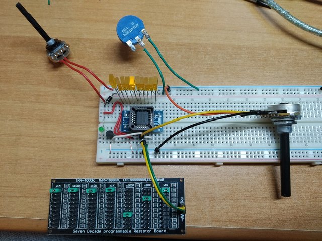
A couple of notes about the build:
- I didn’t have the resistors with the right values and wattage, so I used two potentiometers (set as close as possible to 3.9K) for R1 and R2 and a resistor decade set to 620Ω for R3
- I didn’t have a 2N2905 but rather a Panasonic 2SA1123. I think, since the design is largely independent from the transistor parameters (as long as β is in the hundreds), we can replace Q1 with basically any PNP BJT.
- D1 is a 1N4007. Not a big deal.
- The LM3914V is not a TI original but rather some clone.
- Measurements were taken with my Solartron Schlumberge 7150plus which is in good working order, as far as I can tell, but not calibrated.
Measurements
| Variable | Measured (D1 off) | Calculated (D1 off) | Measured (D1 on) | Calculated (D1 on) |
|---|---|---|---|---|
| V+ | 3.626V | 4V | 4.239V | 4V |
| Vref | 1.2488V | 1.25V | 1.2486V | 1.25V |
| VAD1 | 3.025V | ≈2.8V | 4.857V | V+ + 0.7V = 4.7V |
| ID2 | 0.858mA | 1.28mA | 11.778mA | 12.38mA |
| VD2 | 1.7886V | 2.1V (assumption) | 2.178V | 2.1V (assumption) |
| VEB | 0.6329V | 0.65V (assumption) | 0.7484V | 0.65V (assumption) |
| IR1 | 11.06mA | 11.28mA | 10.875mA | 11.28mA |
| ILED | 11.15mA | 11.58mA | 0.009mA | 0mA (assumption) |
| ID1 | 0.011mA | 0mA (assumption) | 10.736mA | 11.10mA (= IR2) |
| VD1 | -0.698V | -1.2V | 0.6897V | 0.7V |
| ILM3914 | 10.17mA | 10mA (assumption) | 9.732mA | 10mA (assumption) |
| Vout | 0.8523V | 0.7V (assumption) | 3.449V | N/A |
ILM3914 is the current entering the V+ pin of the LM3914V and Vout is the voltage at the output port on the LM3914V at the lit led (in case D1 is off) or any other output port (when D1 is on).
Conclusions
In this post we’ve seen how the application is supposed to work on paper, analyzing the bias points of the various components and understanding what happens in every part of the circuit and gaining some in-deep understanding of how the LM3914 works.
I’m also pretty happy with how close the measurements turned out to be to the calculated values given all approximations we did during the course of the analysis. I think most of the error comes from the fact that I considered a voltage drop across diodes to be the same regardless of the current flowing through them (a simplified model of the real thing) to make it easier to reason about it.
I hope this post was helpful to whom is interested in the LM3914. It certainly was interesting and a great exercise to me to write it: this helped me understanding this application in order to design a display based on it (see this post about the display I’m designing).